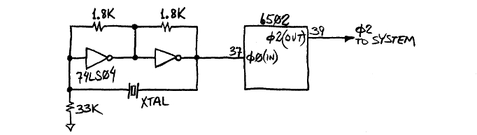
If you're using an old NMOS 6502, you will have to have a square wave input to the Φ0 pin. A commonly used clock-generation circuit went like this:
With this circuit, use a series-resonant crystal to get the frequency printed on it. (The frequency of a parallel-resonant one
will be slightly off in this circuit. To tell whether it's cut and trimmed the be the specified frequency in series- or
parallel-resonant mode, see the crystal's data sheet.)
NOTE about the next two circuits: WDC no longer tests or specifies the gate delays between Φ0 in, Φ1 out, and Φ2 out for their newer 65c02's, and they would prefer that the designer use an external oscillator. All the same internal inverters seem to still be in place though, so I have little doubt that the circuits below will still work fine; but I had to pass the info on.
The CMOS 6502 (65c02) has an on-board oscillator and allows you to connect a crystal and two 47pF capacitors and a resistor, like this:
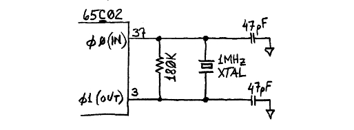
With this circuit, use a parallel-resonant crystal to get the frequency printed on it. (The frequency of a series-resonant one will be slightly off in this circuit.)
If you don't need high speed or accurate frequency, you can even go with just a simple resistor and capacitor, like this:
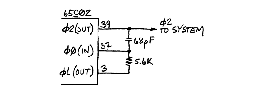
One of our aircraft products designed in 1993 uses this circuit, running at approximately 1MHz, and has proven 100% reliable.
For a standalone oscillator made of discrete components (if you can call the IC a discrete component), this one using a section of a CMOS 74HC14 Schmitt-trigger inverter is the simplest:
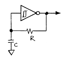
With C=100pF and R=12K, you'll get approximately 1MHz. It puts out a square wave, and will always oscillate, and the frequency will dependably be roughly proportional to 1/(RC), ie, the inverse of the capacitor value times the resistor value. You don't have to worry about it taking off on a harmonic or overtone. The exact frequency will of course depend on the accuracy of the components and the hysteresis points of the inverter's input. The latter is not tightly controlled and guaranteed; so depending on how accurate you want it, you might need to use a trimmer, and even then, the frequency could drift slightly with temperature and power-supply voltage, meaning it still won't match crystal accuracy.
Note: WDC now recommends a separate clock circuit that feeds both the Φ0 input (pin 37 of the DIP) and the rest of the circuit's Φ2, rather than feeding the rest of the circuit from the processor's Φ2 output (pin 39 of the DIP) which would inevitably be slightly delayed from the Φ0 input. WDC also wants a maximum transition time of 5ns, ie, no slower than that; so here's an extra note: A 555 timer is nowhere near fast enough in its rise and fall time, even if you want the frequency in Hz to be super low.
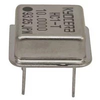
If you need an accurate time base, you will need crystal control of the frequency. There are lots of ap notes and articles on the web about making crystal oscillators (and there's the circuit above), but the most productive path is to just use one of the off-the-shelf oscillator cans that take the space of an 8- or 14-pin DIP (but have only four pins use only the four corner contacts of the DIP socket) and require no external parts, so they take less board space. Going this route will make sure the oscillator will always work correctly for the entire voltage and temperature range, and it's easy to change. The whole oscillator doesn't cost much more than a lone crystal. Here's an enlarged picture of a crystal oscillator that fits in an 8-pin IC socket (two of the pins are hidden behind):
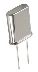
Newcomers to the field often call that a crystal, or think that a crystal by itself will produce a clock signal. No. This is a complete oscillator, with not just a crystal inside, but additionally has the other circuitry inside to make a complete oscillator to produce the desired clock signal. Just a crystal typically looks like this:
Good oscillator design is rather math-intensive (S-plane, anyone?). You might get one going but find out months later when the weather heats up that it doesn't want to work anymore; or you might not have the crystal resonating in the right mode, evidenced by the frequency proving to not be what you thought. If you use the can, the details of making an oscillator that's stable and dependable under all conditions have already been figured out for you. If you're attracted to the fun of making your own, look at it this way: plugging in an oscillator can leaves you more time to work on other parts to make your computer do more.
If you still insist on making a crystal oscillator yourself, a couple of Fairchild ap notes I might recommend are:
HCMOS
crystal oscillators (.pdf)
CMOS
oscillators (.pdf)
An asymmetrical system clock (ie, not high and low for equal amounts of time) may reduce the maximum operating speed of your computer. (If you're not pushing the upper speed limit, don't worry about symmetry.) To get good symmetry on the clock from an oscillator that does not have a symmetrical output, you can start with twice the frequency and divide it by two with a flip-flop, like this:
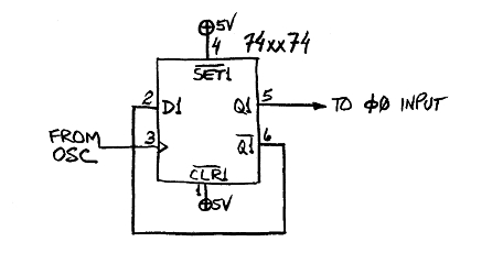
If the clock oscillator's output is 4MHz, the flip-flop's output will be 2MHz. The flip-flop's output will have a 50% duty cycle, because every time the oscillator has a rising edge, the flip-flop's output changes logic state, and the oscillator's falling-edge timing doesn't matter, because it doesn't do anything. Note that the Q1 output will be like a Φ1 or a Φ2 but will be just slightly ahead of the processor's Φ1 and Φ2 outputs. If you need such a signal in the glue logic and gate delays in the glue logic are a problem, this may be a solution. It will probably be more useful in a 65816 system, particularly for latching the bank byte with a '573.
In any case, do not connect a clock source to the Φ2 pin of the 6502 (pin 39 of the DIP), since that's an output. External clocks need to be brought in by way of the Φ0 input (pin 37 of the DIP). (On the 65816, the Φ2 pin is an input, but on the 6502, it's an output.)
If you have a variation like the 6512 which needs a two-phase non-overlapping clock input, see 6502.org forum member gfoot's circuit here
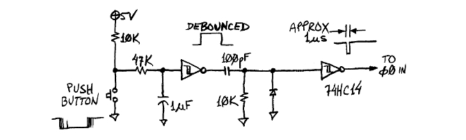
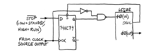
You may someday want to single-cycle the computer so you can see what's on the buses at each cycle. You can't do this with the NMOS 6502 because its internal registers lose data if you slow the clock down much below 100kHz, but you can stop the 65C02's clock with Φ2 high indefinitely, and WDC's '02 can be stopped indefinitely in either phase (ie, with Φ high or low). The diagram below shows a circuit that debounces a button push and produces a 1µs (give or take) down-up pulse every time you push the button. This really is only useful in certain debugging situations where the problem happens immediately (or almost immediately) after start-up. (If it's not soon after start-up, it will take too many button pushes to get there.) It would temporarily replace any other clock source that you have feeding the Φ0 input (pin 37 of the DIP). Note that the Schmitt-trigger inverter must be CMOS, not 74LS14.
Another circuit lets you single-step, IOW, go one instruction at a time, rather than one down-up clock cycle at a time. This is different from single-cycling in that the steps stop on the op codes only, not showing you what happens when operands or data are on the data bus.
The 6502 uses a Φ2 system clock and a R/W (read/write-not) line instead of a RD and a WR line like some other processors use. If you need RD and WR signals in order to use I/O ICs of other processor families, you can do something like the following circuit. (Note: As always, the address bus always tells where the access will occur, but the I/O ICs of other such processor families will depend on RD and WR, instead of directly on Φ2, to tell when the access is valid.)
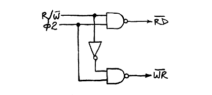
Otherwise, you will connect the Φ2 pins of all the 65-family parts together (the processor having the Φ2 output that feeds the Φ2 inputs of all the I/O chips), and connect the R/W pins to each other the same way. The R/W line will also go to the RAM chips' WE pins. There's no need to take R/W to the ROM as well. Although writing to ROM will cause bus contention without it and possibly high currents, it's definitely within the programmer's power to avoid writing to ROM addresses, so it's not a problem.
If you want to see how fast your creation will go before it starts having problems, instead of buying a whole series of crystals or oscillators at incrementally higher frequencies to try, you can make yourself a variable-frequency oscillator (VFO) as shown in this forum post or the link it contains. Connect it only temporarily for the test and gradually turn the frequency up until you find problems, and then measure that frequency. A frequency counter is best, but you can get within perhaps 5% by measuring the period on an oscilloscope and inverting the number. Then get whatever standard-frequency crystal oscillator happens to lie in the 70-75% area, to make sure you'll have some safety margin for when operating conditions are not ideal (like higher temperature, an additional bus load when you expand the computer, or a slightly lower power supply voltage).
Under good conditions, parts will usually go quite a bit faster than the specifications say; for example you may get 4MHz 65-family parts to run at 7MHz; but they're not guaranteed to meet the specified timing margins anymore, so the 4MHz parts would require faster logic and memory than say 10MHz parts would at the same speed.
2/17/19: Jeff Laughton posted a very simple clock-stretching circuit to replace a RDY circuit,
here. It does not affect VIA timing.
:) Note that the NMOS 6502 does not pay attention to RDY in write cycles; so if you have to use NMOS with something that's slow to write,
this will take care of that. His RDY circuit is here.
74 families & timing <--Previous | Next--> reset circuits
last updated May 19, 2025