
A few basic memory abreviations should probably be defined up front:
Since your memory and I/O are separate from the microprocessor (ie, everything is not on one IC like a microcontroller has), you will need some address-decoding logic to take the address the microprocessor puts out on its address bus and use it to get the attention of the right IC, and normally only one IC at a time. It is good to keep this glue logic simple, for a couple of reasons.
Unfortunately, beginners tend to be repelled by the fact that keeping it simple appears to leave a lot of "wasted" space for I/O. They're sure they need all the address space they can get for memory. After all, the 6502's memory space is super limited already, isn't it? That's the appearance, when you compare to modern PCs that have gigabytes of memory. Keep in mind however that the PC is running many dozens of tasks at once (mine is running 76 at the moment, plus I have well over 100 browser tabs open), uses tons of hi-res graphics, uses object-oriented programming particularly for the GUIs (and OOP tends to take a lot more memory), and bloatware abounds, meaning that for faster time to market, developers use methods that are not memory-efficient, including pre-written software modules that may have a lot of portions that are not needed for the application. I highly doubt that these things will characterize your project and your situation. For a 6502 beginner, 64KB (or even 48KB, or even 32KB) will be an absolutely huge memory space to fill with code; so I'd say you're not in any danger of running short. I've been using the first diagram below on my workbench computer for 27+ years, and the only thing I've ever needed more memory for is large data arrays, never code.
The more obvious reason to keep your address decoding simple is just to minimize the number of parts and connections and the work required to build it, as well as the board space. The other reason beginners often miss is that it takes time to get the signals through each logic level. It is not instant, especially when it involves a connection that is made outside the IC. The time required to get the signal through is called "propagation delay," and is listed in the timing specifications of the various logic ICs. As the glue logic's propagation delays add up (especially from cascading logic levels), a smaller and smaller portion of a microprocessor clock cycle is left for memory or other ICs to deliver data (if you're reading it) or latch onto data and put it in the right place (if you're writing to it). At 1MHz you can get away with some pretty sloppy timing, but the delays will have to be reckoned with as speeds increase.
A few things to note about the propagation delays listed in the data sheets:
For beginning builders, I might recommend the 74HC (or perhaps better, 74HCT) logic family. It is generally (but not always) a hair
faster than 74LS. (There's a forum discussion on that here.)
There are others that are faster and have stronger output drivers like 74AC and 74ABT, but faster can sometimes cause problems for
the beginning builder (and few of the parts are available in 74ABT anyway). I would not recommend 74LS or 7400 as these give no
real benefits to offset the disadvantage of their greater power hunger and the heavy loads their inputs present.
Fairchild has some applications notes which might be of interest: (Note, 12/27/19: Since ON Semi took over Fairchild, they took down these ap. notes. I asked them to re-post some others and they did, and now I've asked them to re-post these too, but I've waited many months; so here are archive.org links to them)
Do not use 4000-series logic for address-decoding! It is extremely slow, especially at 5V and less, and is best saved for when you need to operate at higher voltages (like 12V) and don't need the speed.
If you later want to get into higher speeds, refer to the section, "Construction: Avoiding AC-Performance Problems."
Note that 100ns memory is not fast enough for 10MHz on a 6502! It's only a slight oversimplification to say that the 6502 basically does a memory access in half a cycle, meaning 50ns @ 10MHz, 500ns @ 1MHz, etc., and some of that time will be taken up by glue logic, set-up times, etc., leaving less than you might think for the memory itself. In fact, the Apple II did two memory accesses per cycle, two million per second at 1MHz, with the video accessing the memory during the first half of Φ2, and the processor during the second half, interleaving, so both could access the same memory at the same time at full speed, with no conflicts. Anyway, speed is not just the inverse of the access time.
To expand on the scenario above, consider 100ns memory (let's say it's ROM, so we can leave Φ2 out of it) and a 10MHz 6502. One period at 10MHz is 100ns; but from there you have to subtract the specified address setup time (tADS, 30ns for a 14MHz 6502) and the read data setup time (tDSR, 10ns for a 14MHz 6502) and probably some address-decoding logic time, let's say 10ns but it will depend on your circuit and how fast your logic is, leaving you with about 50ns for the ROM at 10MHz. If you're running it at 3.3V, the specs say you need to take off another 15ns, leaving you with ROM that can dish up the data in 35ns @3.3V. That's if you want to be sure the product will always work. It's nice to know that parts are usually faster than the guaranteed worst case; but for production, you can't assume they always will, because at any time the suppliers could give you slower parts that are still within spec and they won't work at your speed and it won't be any fault of theirs!
Each part's data sheet will have the timing diagrams and timing specifications. Don't ignore them!
BTW, you must capitalize the M in "MHz." If you don't, at 1mhz, it would take a thousand seconds for one cycle! When the letters are used in powers of ten, "m" stands for "milli," ie, "x10-3," whereas "M" stands for "mega," ie, "x106." There are 1,000,000,000mHz in 1MHz.
There's more in the section, "74xx Logic Families and Timing Margins." I must also point
out Jeff Laughton's excellent animated, drawn-to-scale (unlike most in data sheets), visualizations of timing margins, in the forum
topic "Timing Diagrams. Visualizing 65xx Timing."
These .gif's help understand what timings are constant and what varies with clock speed.
Phase-2: the conductor
On the 6502, data transfers between ICs are coordinated by the Φ2 clock signal. The symbol used is the Greek letter phi (not the diameter symbol, nor the crossed numeral zero, nor the empty-set character, although I am not able to get the font I want for the character here either; the phi has the line going through it vertically, not at any significant slant). "Φ" is pronounced "fi," rhyming with "fly," or, less-preferred, "fee," rhyming with "flea;" but what it stands for here is "phase," and it's just as easy to say "phase two," like "gate one" for the 74xx138's G1 input. This clock is not for reading time of day but instead is a timing coordinator square-wave signal that typically runs at a constant frequency.
Unlike many other processors, a "cycle" on the 6502 consists of only the Φ2-low time followed by the Φ2-high time, in that order. The falling edge of Φ2 starts the next cycle. The 6502 does mostly internal operations in the first half of the cycle when Φ2 is low, and its bus accesses (reading or writing) when Φ2 is high. So for example at 1MHz, one cycle takes only one microsecond, unlike many other processors where they really mean an instruction cycle or a machine cycle, terms which are not used with the 6502. The 6502's bus cycle and a clock cycle are the same thing. Instructions take anywhere from two to seven cycles (or clocks) each, averaging around four, a little less if you're doing mostly zero-page operations, or a little more if you're doing lots of indirect and indexed operations.
The Φ2 frequency on a 6502 computer might be anywhere from 100kHz for ultra-low-power systems to 20MHz or more for the highest performance you can get from a 6502 with separate ICs for memory and I/O (as opposed to a microcontroller where everything is in the same IC and the buses don't have to go offboard). If your first aim is for a couple of MHz or less, particularly with slowish parts like a 2MHz processor and 74HC logic, your chances of initial success will be excellent. Higher frequencies and faster parts require better construction in order to avoid certain problems. We will get into construction and into clock generation and distribution later.
Address-decoding logic can be much simpler than we often see in hobbyists' designs. The 6502 has memory-mapped
I/O, meaning that I/O and memory are treated and addressed the same way, giving extra flexibility and efficiency of program code and
allowing a nearly limitless amount of I/O. With only a 74HC00 quad NAND gate in a 14-pin DIP, you can do the address decoding
for 32K of ROM and 16K of RAM and as many as ten I/O ICs like the 6522 and 6551. Consider the circuit:
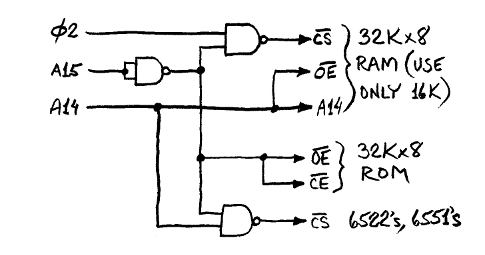
(The NAND on address line 15 is only used as an inverter. You could also feed A15 into only one input and connect the other input to Vcc.)
  6522  VIA   has CS1, CS2
  6551  ACIA  has CS0, CS1
  27256 EPROM has OE,  CE
  62256 SRAM  has OE,  CS  But note!  Tying the SRAM's OE to A14 effectively makes it a 16KB with a CS2!

  A13 -------> CS1 of VIA1
  A12 -------> CS1 of VIA2
  A11 -------> CS1 of VIA3
  A10 -------> CS0 of ACIA1
  A9  -------> CS0 of ACIA2
  A8  -------> CS0 of ACIA3
  A0-A3 -----> RS0-RS3 of VIAs
  A0,A1 -----> RS0-RS1 of ACIA1
  A2,A3 -----> RS0-RS1 of ACIA2 & ACIA3

  IC:   address: (the "$" means "hexadecimal," or base-16)
  RAM   $0000-3FFF (only 1/2 of 32KB available.  Writing to I/O also writes to the upper half of RAM, but
                                                 you can't read it back since it would interfere with I/O.)
  ROM   $8000-FFFF (all 32KB available)
  VIA1  $6000-600F
  VIA2  $5000-500F
  VIA3  $4800-480F
  ACIA1 $4400-4403
  ACIA2 $4200, 4204, 4208, 420C
  ACIA3 $4100, 4104, 4108, 410C
  (and up to four more I/O ICs could be added)
Note, to address a forum controversy: I've been using this scheme at least since the early 1990's, and published it on the forum in 2000. It's not necessarily brilliant; but all the earlier quad-NAND-gate schemes I've seen are different from mine. So although I "invented" it, someone else may have done it first and I just wasn't aware of it. The web hardly existed at the time.
Propagation delays ought to be kept short particularly for Φ2; and this circuit does that very well, having only one NAND gate delay between the 6502's Φ2 output and the RAM's CS.
Each 6522 VIA has a positive-logic chip select labeled CS1, and a negative-logic chip-select-not labeled CS2. The 6551 ACIA has CS0 and CS1. All the CS pins are connected to the output of one of the NAND gates, and each of the CS pins goes to a different address bus bit. Leaving the top two address bits (A14 and A15) for the 74HC00 to select 16K sections of memory, and leaving the bottom four address bits (A0 through A3) for the register-select pins (labeled RSx) on the 6522's and 6551's (as well as A0-A3 of the memories), we have A4 through A13 available for the CS pin of ten different I/O ICs that have their own Φ2 input.
Schemes like this mean that each I/O IC's address range is mirrored in other places in the address map. Normally you'll want to use the address that is not shared with others, so you can avoid addressing more than one IC at a time. In practice it has proven to be no problem at all. In the case above, the unique address ranges you would use are as follows:
62256 SRAM: $0000-3FFF (binary 00xxxxxxxxxxxxxx) (There are no 16Kx8 SRAMs, so here we use half of a 32Kx8.) 6522 VIA1: $600x (binary 011000000000xxxx) 6522 VIA2: $500x (binary 010100000000xxxx) 6522 VIA3: $480x (binary 010010000000xxxx) 6551 ACIA1: $440x (binary 010001000000xxxx) 6551 ACIA2: $420x (binary 010000100000xxxx) 6551 ACIA3: $410x (binary 010000010000xxxx) 27256 ROM: $8000-FFFF (binary 1xxxxxxxxxxxxxxx)(Note: I had an error in this table, from mixing up connection ideas, and forum member adrianhudson caught it and brought it to my attention on 5/2/22. Fixed.) Address bits 4, 5, 6, and 7 can be used for additional I/O ICs, which is why they're not also shown as x's here.
This is approximately what I have in my workbench computer, with the possibility of four more I/O ICs each having a CS, a CS, and a Φ2 input. Although you wouldn't normally address more than one at a time, there exists the possibility of writing the same byte to two or more VIAs (or ACIAs) at the same time by setting two or more of the appropriate A4 through A13 address bits high at the same time. A possible reason would be to set matching I/O bit directions, baud rates, etc. with fewer instructions. (Just don't try to read more than one at a time, or you'll get bus contention and no worthwhile outcomes!)
Notice in the diagram above that Φ2 is involved with the RAM select but nothing else. You must have a way to make sure RAM cannot be written when Φ2 is low! This is one way to do that. Looking at the 6502's timing diagrams in the data sheet, you will see that the address lines are not guaranteed to be valid and stable before the R/W goes low; so it is possible to write to unintended addresses. With an extremely simple program that you might use to see if the computer is working at all, the other addresses it writes to might not be ones you're using yet; but soon they will be, and you'll start writing garbage over your variables, or your stack space, or even your program, when you still need those areas to remain intact. The result will likely be a crash.
(If we really needed the fastest RAM access time, we would need to make it a little more complex to give the RAM a head start in getting selected when Φ2 is low, and then not enable the writing especially until Φ2 rises; but the speed limiter in our basic computer here will be the access times of commonly available (E)EPROMs anyway, not RAM, so we will keep it simple for now. If you want to look into it further, see BDD's diagram here.)
The VIAs and ACIAs have their own Φ2 input, and the address decoding must provide the appropriate valid chip-select before the Φ2 rising edge. I know from experience that the VIA will not work if the CS waits for the Φ2 rising edge. (I found out in about 1986, then years later had to use the trick shown near the bottom of this page when I used a pair of 6522's in a Commodore 64 I/O expansion board, the C64 not giving an early select signal.) Do not bring Φ2 into these ICs' CS logic like the circuit above does for RAM.
Φ2 is not needed for ROM on the 6502, since anytime a ROM address is put on the address bus, it's to read from ROM (not write), and the address will be stable from before it's needed until after it's no longer needed. This holds true even though the ROM does not have a Φ2 input pin. Omitting Φ2 from the ROM CS does not produce any danger of overwriting needed data anywhere. (If you later go to the 65816, you may need to bring Φ2 into the ROM's output enable, to avoid bus contention when Φ2 is low since the processor will be trying to force the bank address onto the data bus while the ROM will be trying to force its output data onto the same bus at the same time. Use of the usual recommended '245 bus trasceiver (or equivalent function in programmable logic for example), which is disabled during Φ2 low, will avoid the bus contention.)
Here's a variation that gives 32K of RAM and 16K of ROM (instead of vice-versa like the one above):
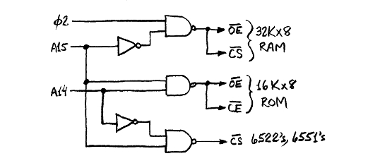
Then you get RAM from 0000-$7FFF, I/O from $8000-$BFFF (again up to 10 I/O ICs can be accommodated with this decoding method), and ROM from C000-FFFF. Michael on the 6502.org forum shows another way using a single '139, here (although you'll need another IC for reset).
So why 3 VIAs and 3 ACIAs, you ask? The section "Expansion Buses and Interfaces" mentions many of the things the VIAs are used for. As for the ACIAs, two would be plenty now; but the original idea was to have one for a link to the PC that I use for software development for its full-featured programmer's text editor (MultiEdit) and hi-res monitor and disc drives and full keyboard, another ACIA for a wireless link or for MIDI (musical instrument digital interface), and the third one for a cassette tape modem which has become purposeless now 20 years later since serial EEPROMs and flash memories are tiny and have become so cheap and are much faster and store far more data than a whole box of cassette tapes could. I originally envisioned using all three ACIAs at once.
To get 32KB of ROM and almost 32KB of RAM, you can use Daryl Rictor's memory decoder IC that he sells for $7. It's a pre-programmed 15ns GAL22V10 24-pin programmable-logic IC that gives the upper 32KB space to ROM, and gives the lower 32KB to RAM except that it takes page 2 ($0200-$02FF) out for four I/O ICs.
Otherwise, for decoding more address bits without making the total propagation delays too long, consider using the 74HC521 (or '688—same thing) 8-bit identity comparator, instead of cascading 74HC138's. Suppose you wanted 64K of contiguous RAM minus 256 bytes for I/O at addresses $FE00-FEFF (ie, page $FE) and 256 for ROM at $FF00-FFFF (ie, page $FF, just enough for a reset routine to load a program into RAM from some sort of mass storage). Consider the circuit:
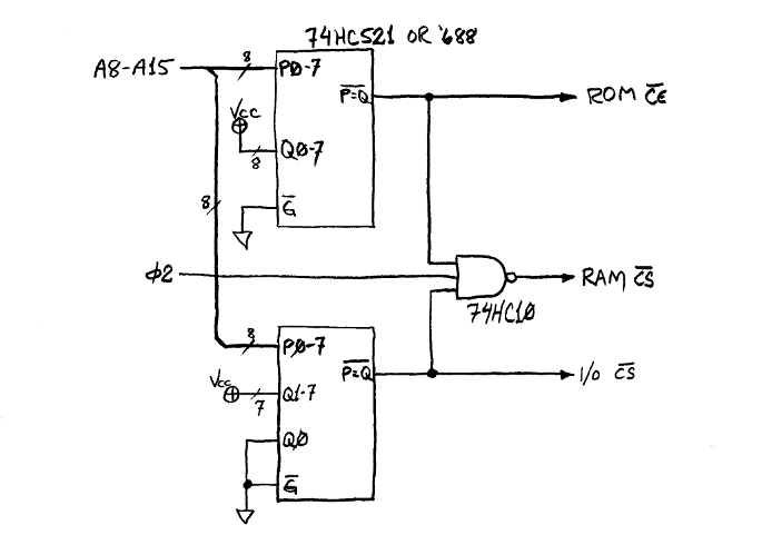
This eliminates the conflict over how much RAM and how much ROM to have. What's normally in ROM with the previous circuits gets loaded into RAM from mass storage instead, by a short routine in the tiny ROM space between address $FF00 and $FFFF, and the remainder of the RAM is available, whether that means 2K or 60K left. With no further address-decode logic, it leaves room for four of the I/O ICs mentioned above.
There's discussion with some good points on other simple address decoding methods in the forum topic "I think I finally have my decoding down. Suggestions needed." Forum member "Michael" who posted several times in that topic also has a simple (two-IC) circuit to get 32K of RAM, 32K (minus 256 bytes) of ROM, and 256 bytes of I/O space, here, and a configurable one, here.
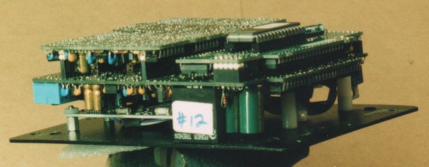
So how few parts is it possible to get away with for a 6502 computer (without using a 6502-based microcontroller)? Here is one I designed to control one of our products in 1993, a high-end intercom for private aircraft. We kept selling it for nearly 15 years.
It has the processor, RAM, ROM (on the back), a 74HC00 for glue logic, an 8-pin serial EEPROM to store custom set-up defaults, and a 65c22 VIA for I/O. (The 6522's synchronous-serial port is used along with shift registers on the main board to get a lot more I/O than meets the eye.) Here's the inside of the main box of that intercom. Can you see the CPU board sitting there on top?
In the early stages of development (fall of 1992), I considered several different microcontrollers for the job. Many had severe
limitations for our application. One manufacturer actually told us that we basically were too small for them to be interested in
our business. We settled on one of the Motorola 68HC11's, but then found out that unfortunately the version we needed with EEPROM
and lots of EPROM was on allocation and not easy to buy. As it ended up, we just went back to a discrete 65c02 computer on its own
board. Our cost for parts and labor was approximately what the HC11 was going to cost anyway—it just took a little more room.
(Again, the EPROM is on the back, making the board smaller.) Soon after, Microchip PIC16's took a large market share. The
processor in them is really lousy compared to the 65c02, but they have a lot of variations, features, I/O, built-in processor support like
reset circuit and watchdog timer, etc., have good technical support with lots of ap. notes and free assembler etc., and are inexpensive and
widely available. This makes the PICs well suited for tiny jobs; but otherwise they have severe limitations.
Intro: Why 6502? <--Previous | Next--> memory map requirements
last updated Sep 4, 2025