There are dozens if not hundreds of I/O (input/output) ICs that can be used on the 6502 bus, but the two most common ones you'll find used by hobbyists are the 6522 VIA (Versatile Interface Adapter) and 6551 ACIA (Asynchronous Communications Interface Adapter). (Pronunciation: Say "vee-eye-ay." A via, lower-case, pronounced "vee-uh," is a hole in a PC board that's only there to connect the copper of one layer to the copper of another layer at that point.)
The 6522 (and 65c22, ie, CMOS) VIA has:
The 6522 VIA (above) has significant advantages over the 6520 or 65c21 PIA (peripheral interface adapter). It has two multi-mode timer/counters and a synchronous-serial port which are absent in the '21. Another disadvantage of the '21 PIA has compared to the '22 VIA is that access to the data-direction registers on the PIA is only indirect, requiring more instructions, making it pretty clumsy to emulate open-drain outputs when needed. The way to to it is to set the output register's bit to a 0 and then change the data direction, so that even in "output" mode, sending a 1 is accomplished by making the pin an input so the external pull-up resistor can bring the line up. (The output register bit is left as 0.) This is valuable for example when bit-banging an I²C or PC keyboard interface. The '22 VIA is much more efficient at this.
The 6551 ACIA (and 65c51, ie, CMOS) has everything you need for a complete RS-232 (TIA-232) link except a crystal and the line drivers and receivers. It includes the onboard baud-rate generator (unlike the 6850 which lacks it, which is why I do not recommend the 6850) and five handshake lines: RTS, CTS, DSR, DTR, and DCD. My RS-232 primer tells about it. You might not think you have any use for an "antique" RS-232 serial port connection, but UARTs (including this ACIA) are used even for interfacing to some modern displays. RS-232 is still used in industrial environments where they need a longer range than you can get with other things like USB which are more oriented toward consumer electronics and are more "black box" and not as hobbyist-friendly. The ACIA can also be used for RS-422 and RS-485 which use different line drivers and receivers but may use the same communications protocol.
Traditionally, it has been the 6551 or 65c51 (ie, CMOS version) that have been put on the 6502's bus to get asynchronous serial communication. I've used the 65c51 for decades and never had any trouble with it. I could wish that a couple of the functions had been separated rather than being controlled by the same bit in the command register; but it hasn't been any real problem in my applications, and separating them would have required adding another register-select pin. The WDC W65C51 (which I have not used, but it's the only '51 still in production) has a serious bug, described further down, with links to workarounds. However, these, and possibly the absence of FIFOs (First-In, First-Out, multi-byte buffers) for transmit and receive, have shifted the 65 community's favor toward other UARTs, one of those having been the 28L92. Unfortunately that one has recently been discontinued. See this forum topic, which also gives alternatives that are partially compatible. (I don't particularly think of the lack of a FIFO in the '51 to be a problem, because the 6502 has such good interrupt performance, and the interrupt overhead you have to go through for each byte received or transmitted is minimal, unlike the situation with many other processors that truly needed the UART to have FIFOs.)
In sections 10 ("Expansion Buses and Interfaces") and 22 ("circuit potpourri"), and in my forum post here, I tell about synchronous-serial interfaces, one of them being the popular SPI. The MAX3100 is a 14-pin UART that interfaces to the processor through SPI. I've tried it and like it so I will probably use that one in the future. It has 8-byte transmit and receive buffers and takes less board space than the 6551. Part of its design is specifically to also be IrDA-capable (for infrared communications). The MAX3110E is the same thing with line drivers and receivers built in, and it doesn't need any support parts like the popular MAX232 line driver/receiver IC does.
The 65SPI I/O IC, designed by Daryl Rictor, provides direct and complete SPI support in a 65-family IC. There's a ton of I/O ICs on the market that interface by SPI, and his 65SPI IC is a great way to interface to a lot of them at once. For example if you want to try USB later, Maxim has USB ICs that take care of all the internal details and interface through SPI and require very few parts.
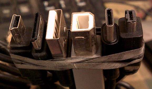
And since I mentioned USB, another simple-ish way to get USB is through adapters, which you can get here, here, here, here, and probably several others. Here is a tiny module that interfaces to your project by UART or I²C and acts as a USB controller, with all USB software already onboard. Myself, I hate USB for several reasons. The USB 2.0 spec is 650 pages. Just the part about transferring power through it is over 100 pages! It is not hobbyist- or workbench-friendly at all. You cannot make up your own cables, or troubleshoot it with an oscilloscope, or write a driver that fits in an 8-bit computer's memory. The spec precludes a hand-held device from being a USB controller. It also cannot go over 16 feet without repeaters. Further, the name is short for "Universal Serial Bus;" but how can they call it a bus if normally one port goes to only one device? And how can they call it "universal" when there are eleven kinds of plugs, plus male and female of each? Here are six I picked up off my desk to take a picture of:
For detailed information on how to use the following and other ICs, consult the data sheets available on 6502.org's
data sheet page. There have been many different 65-family
I/O ICs, but the ones listed above are being made today in higher speeds (14MHz or more). Older ones I am aware of are the
There are lots of non-65-family I/O ICs you can connect to the 6502's buses, but they may require slightly more logic, for example if they have RD and WR inputs. The simple circuit for deriving those two signals is shown near the end of the Clock Generation section.
You can also use something like 74HCxxx output latches (as output ICs) and input buffers (as input ICs) on the bus, but it's more work and gets you less return on investment. I started out that way on my first home-made computer, and although it worked, it was a huge amount of labor to build and wasn't really useful for anything.
If you have questions or problems, post them to the forum (preferable) or email me directly at wilsonminesBdslextremeBcom (replacing the B's with @ and .). I check the email countless times a day and respond quickly.
My main workbench computer uses the first VIA for:
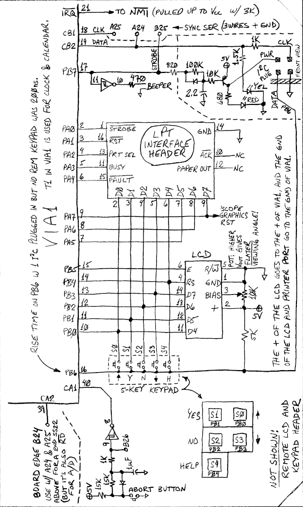
The last list above was also given in the section "Expansion Buses and Interfaces," but
without the diagram. My next one will make more efficient use of the VIAs, allowing even more to be connected.
Many of the tips in my "Tip of the Day" topic on the 6502.org forum are about the 6522 and 6551.
Some on the forum have suggested using a PIC16 microcontroller for I/O including the SPI, I²C, A/D converters, PWM, etc.,
going through the PIC's PSP (parallel slave port). You can put it right on the processor's data bus, but it's slower than
something like a 6522 because you have to for example write the data to the PIC, then give it enough time to see it and do something
with that info, then come back again and tell it what it's supposed to do with that data, then again give it more time to process it,
maybe polling it in between to see when it's ready for the next thing, and so on. If you want to read data, you'll tell it what
you want to read, give it time to get that data ready to output, come back later to read it, etc.. For this reason, it would be
better to use the PSP only if the amount of data is rather small compared to the job the PIC will be doing with it. See
Microchip's ap. note AN579 (.pdf), about
using the PSP. You would of course have to have a way to program the PIC. (Note, Mar 2019: I have
been informed that there are newer PICs that don't require such a tedious way of working the PSP anymore.)
Here's a little extra info on the 1.8432MHz input for the 6551 ACIA, typically used for RS-232, for which I have a primer here. (Note that the 1.8432MHz is separate from the Φ2 rate. The 6551 still needs a Φ2 signal from the processor, and its frequency does not need to be related at all to the 1.8432MHz used to get the data rates.) The 6551 also allows connecting a crystal directly to the XTAL1 input and XTAL2 output pins (pins 6 & 7 of a DIP, respectively) as shown in the following diagram (but don't try an RC timebase—it won't be accurate enough).
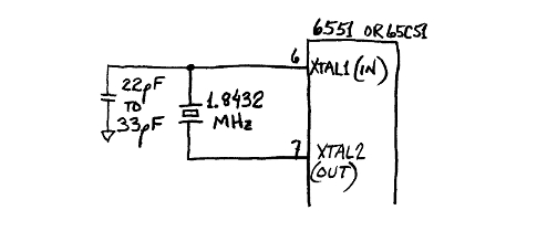
Different manufacturers may have slightly different recommendations. You can check their data sheets if you really want to do it their way, but the above diagram will probably work with most of them. WDC recommends a 1M resistor across the crystal to bias the XTAL1 input.
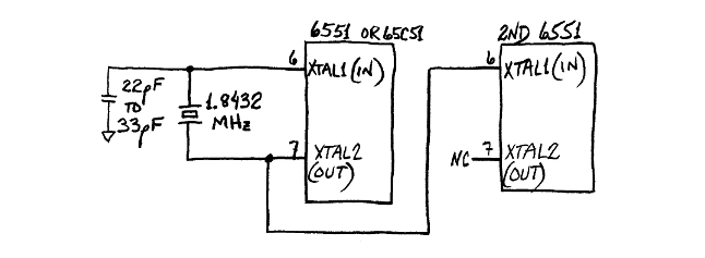
If you have more than one 6551, you can connect the XTAL2 output of the first one to the XTAL1 input of subsequent ones as shown
here:
If you prefer to use a standard 1.8432MHz crystal oscillator can, just connect its output to the to the XTAL1 inputs (pin 6 of the DIP) of your 6551(s).
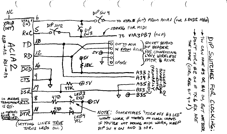
The 6551 does not necessarily have to run on this crystal frequency. MIDI (Musical Instrument Digital Interface) for example, runs at 31.25 kbps. To get that, connect a 500kHz square wave to the XTAL1 input. Then in software, set the ACIA to use the clock ÷16 for the transmit baud rate generator, and set the receive clock to be the same as the transmit clock. So where do you get the 500kHz? One easy way to get it is from PB7 of one of your 6522 VIAs. Here's what I have on my workbench computer, showing the DIP-switch clock options for ACIA #2. This is actually one of the 3x5" pages in my mini ring binder:
The code to set it up for MIDI would be as follows:
     LDA  VIA_DDRB
     ORA  #80H		 ; Make VIA PB7 an output for outputting
     STA  VIA_DDRB	 ; the square wave from timer 1 (T1).

     LDA  VIA_ACR
     ORA  #C0H		 ; Free-run T1 with output on PB7.
     STA  VIA_ACR	 ; (Don't enable T1 interrupts though.)

     LDA  #3
     STA  VIA_T1CL	 ; Write 3 to T1CL for 5MHz Φ2.  0 if 2MHz.
     LDA  #0
     STA  VIA_T1CH	 ; Write 0 to T1CH.  (Do T1CL first.)

     STA  ACIA_STAT_REG	 ; (Software reset of ACIA)
     LDA  #1011B
     STA  ACIA_COMM_REG	 ; No parity or echo, TX & RX enabled, no IRQ.
     LDA  # 10010000B	 ; 2 stop bits, 8 data bits, RX clk=TX clk,
     STA  ACIA_CTRL_REG	 ; TX clk=1/16 of XTAL1 input frequency.
For the 65c02, it can be shortened by three lines by using TSB and STZ, or by four lines if your I/O is in ZP and you start with SMB7 above.
You can also have the receive clock and transmit clock different, with the transmit clock on the XTAL1 input and the receive clock on the RxC input (pin 5 of the DIP). The diagram above shows this too.
Similar to the above, you can get much higher data rates out of the ACIA, still under software control—it's just that it won't be from the 1.8432MHz crystal and the ACIA's own baud-rate generator. Instead, use the VIA's T1 in free-run mode toggling PB7 on every timeout with no further attention from the processor, and select the rate by writing to T1CL and T1CH as shown in the code above. The ACIA data sheet says the ACIA is good to 125kbps, and I suspect that that's rather conservative. 115200 is a standard bit rate, and you can get it by running the system on a Φ2 rate of 7.3728MHz (which is a standard crystal & oscillator frequency) and storing 0 in T1CL and T1CH. Then you can also get all the other standard speeds by writing different values to T1.
Writing    0 to T1 gives 115200 bps.  (These apply to a Φ2 rate of 7.3728MHz.)
Writing    2 to T1 gives  57600 bps.
Writing    4 to T1 gives  38400 bps.
Writing    6 to T1 gives  28800 bps.
Writing  $0A to T1 gives  19200 bps.
Writing  $0E to T1 gives  14400 bps.
Writing  $16 to T1 gives   9600 bps.
Writing  $2E to T1 gives   4800 bps.
Writing  $5E to T1 gives   2400 bps.
Writing  $BE to T1 gives   1200 bps.
Writing $2FE to T1 gives    300 bps.  (The 2 goes in the VIA's T1CH.)
The bit rates shown here are exact. With adjusted T1 values, it would also work to run Φ2 twice as high, at 14.7456MHz which is another standard crystal & oscillator frequency. Other Φ2 rates would work too; but to hit the standard RS-232 bit rates exactly (or at least with an acceptable error of about 1% or less), you'll have to work around the poor granularity caused by the big jumps in PB7 output frequency that result from single-step adjustments in T1 value when it's near 0.
Added Oct 7, 2018: GGLabs' GLINK232 aftermarket board for the Commodore 64 and 128 uses a 65c51 with a 3.6864MHz (ie, double speed) crystal so all the baud rates are twice what the ACIA's data sheet says. According to this forum post, even early 6551's have been successfully used this way in several designs. I'll update this when I find out more.
My article on simple ways to do multitasking without a multitasking OS has sample code (about 70% of the way down the page) for doing the required delays to get round the above bug while still allowing the computer to do other things at the same time, so that you don't have to tie everything up to run delay loops.
Edit, 2/8/19: I think 6502.org forum member GaBuZoMeu has the best solution yet: Use the 51's pin 5 (if in DIP), the x16 clock, as an output to drive a VIA's PB6 for its T2 to count pulses and generate an interrupt. The T2 latch value does not need to change with Φ2 rate nor with baud rate.
Edit, 12/18/23: Forum member John_M had another idea, which was that if you have a '51 RxD (or other UART RxD input) that's free, you could use it to monitor the TxD output of the buggy chip, and use the 'RxD register full' interrupt to indicate that the byte has been sent.
Note that many of the 65xx parts can operate far faster than specified— it's just that they're not guaranteed to. 6502.org forum member BillO has run CDP65C51AE2 (2MHz?) 65c51's up to 20MHz, connecting the Φ2 input to the processor's clock input (not its Φ2 output) so they're both driven from the same source, and with really fast chip select. It's unclear who the actual manufacturer is, since apparently at least five different ones used the same prefixes and suffixes.
I might mention here a potential problem that's relatively simple to prevent but may be difficult to troubleshoot. When
servicing 6551 ACIA interupts for simultaneous transmission and reception, remember that reading the status register clears
the interrupt, but the interrupt could have been caused by both TX register empty and RX register full at the same time. If your ISR
ends before finding all the interrupt causes, it may, for example, find the receive register full, service that, and then exit thinking it's
done, when in actuality the transmit register emptied before you read the status register and it's waiting for the next byte. Now the
IRQ line is false and the issue will never be addressed, and transmission will come to a halt. If more than one thing in the same IC
could need service, make sure the ISR doesn't stop before the whole job is done. This is from my
tip #14 in my
"Tip of the Day" column.
I offer a bit-I/O module on the front page of this site with 8 input bits and 8 output bits, intended for where bits are twiddled or
tested independently of others in a group. It's faster and more code-efficient than doing it with a VIA (although it's intended to
augement, not replace, the VIA). It requires neither RMW instructions, nor AND nor ORA instructions, nor altering A,
X, or Y. It can be used as an IC, but takes only as much board space as a 16-pin DIP.
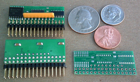
Overall size is 1.600" x 0.680", not including the pin header. Data sheet is here (.pdf). It has the circuit, sample code, interfacing ideas, and more. The idea came from the book "Advanced 6502 Interfacing" by John M. Holland, first edition, pages 37 & 53. Use the information in the data sheet to make your own on your board, or you can buy mine as a module to plug into your board.
Note that there are lots of I/O interfacing ideas on the "potpourri"
page, and I will keep adding more as time permits. It includes links to code to work the various circuits.
Custom PCBs <--Previous | Next--> Displays
last updated Dec 18, 2023